The world of technology is constantly evolving, and researchers are always on the lookout for materials that can revolutionize electronic components. Two-dimensional (2D) semiconducting materials have emerged as a promising candidate due to their distinct optoelectronic properties. These materials offer advantages such as ultra-thinness and tunability, making them highly sought after for the development of advanced electronic devices.
Despite the potential advantages offered by 2D semiconductors, there are challenges in effectively interfacing these materials with gate dielectrics. Interfacial traps often form, leading to rapid degradation in the performance of transistors. Researchers at institutions like King Abdullah University of Science and Technology (KAUST) and Soochow University have been working tirelessly to address these challenges and unlock the full potential of 2D semiconductors.
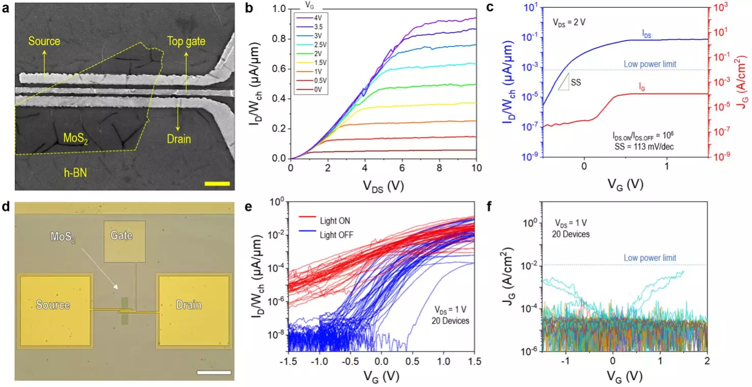
In a recent study published in Nature Electronics, researchers introduced an innovative approach that could revolutionize the fabrication of transistors based on 2D semiconductors. By utilizing hexagonal boron nitride (h-BN) dielectrics and metal gate electrodes with high cohesive energy, the researchers were able to significantly improve transistor performance. The use of platinum (Pt) as an anode in particular proved to be effective in reducing dielectric breakdown and leakage current.
The research team led by Yaqing Shen and Prof. Mario Lanza fabricated over 1,000 devices using chemical vapor deposited h-BN as dielectrics. By incorporating high cohesive energy metals like Pt and tungsten (W) into their design, the researchers were able to achieve a high dielectric strength of at least 25 MV/cm. This breakthrough paves the way for the use of CVD h-BN as a gate dielectric in 2D transistors, challenging conventional beliefs about its effectiveness.
The researchers meticulously cleaned substrates, patterned electrodes, and transferred materials to create transistors with improved reliability and performance. The van der Waals interface between MoS2 and h-BN in their transistors played a crucial role in minimizing defects and enhancing gate control. The team’s findings highlight the importance of selecting the right metal electrodes to enable the effective use of CVD h-BN in field-effect transistors.
The approach developed by Shen and her colleagues has shown highly promising results, significantly reducing leakage currents and improving dielectric strength. With the potential to facilitate the development of reliable solid-state microelectronic circuits and devices, this research opens up new possibilities for the use of 2D materials in the electronics industry. As other research groups begin to explore similar approaches and materials, the future of 2D semiconductor-based devices looks brighter than ever.
As the research progresses, the team plans to delve into developing ultra-small, fully 2D transistors to push the boundaries of Moore’s Law. The journey towards unlocking the full potential of 2D semiconductors is far from over, but with innovative approaches and collaborative efforts, researchers are paving the way for a new era of electronic devices that are thinner, faster, and more reliable than ever before.

