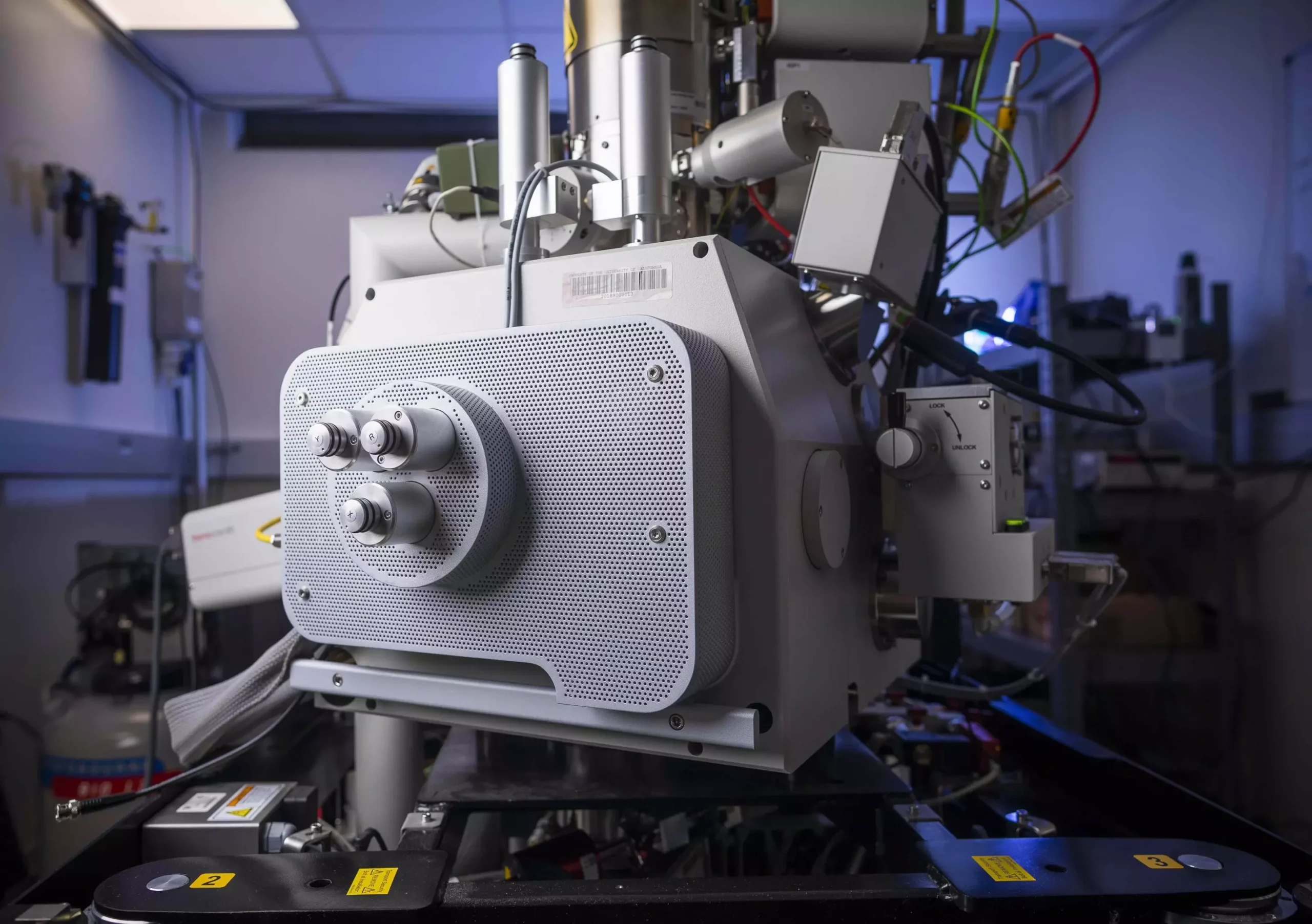
The realm of semiconductor technology is both fascinating and essential to modern electronics. At the heart of many electronic devices lies the dynamic behavior of electric charges, particularly the movement of photocarriers. A recent study conducted by researchers at the University of California, Santa Barbara (UCSB) marks a significant milestone in our understanding of this phenomenon. For the first time, they have successfully visualized the journey of electric charges traversing the interface of two different semiconductor materials, utilizing innovative techniques that could redefine semiconductor theory and application.
Historically, the behaviors of photocarriers have been discussed extensively in theoretical frameworks. Professors and researchers have relied heavily on indirect measurements to infer the behavior of charges in semiconductor materials. However, the research team led by Bolin Liao at UCSB has introduced Scanning Ultrafast Electron Microscopy (SUEM), a novel approach allowing them to finally witness the elusive process of charge movement. “There are a lot of textbooks written about this process from semiconductor theory,” Liao states, emphasizing the gap between theory and observation in the field. The findings from this groundbreaking study are shared in the Proceedings of the National Academy of Sciences.
To put the research in context, it’s vital to grasp the concept of photocarriers. These carriers emerge when semiconductor materials are exposed to light, such as in solar cells. The exposure excites electrons, prompting their movement and creating a flow of electricity. However, these electrons typically shed a significant amount of their energy rapidly, losing valuable potential in just a few picoseconds. As a result, although their “hot” state holds promise for efficient energy use, it also brings complications, such as excess heat production that can detract from device performance.
Understanding the behavior of these hot carriers as they migrate between different semiconductor materials is crucial, especially at interfaces known as heterojunctions. These heterojunctions are pivotal in various applications, including photovoltaics, lasers, and sensors, governing how charge carriers function and interact.
Professor Liao and his team turned their attention to a heterojunction composed of silicon and germanium, two ubiquitous semiconductor materials that demonstrate immense potential for applications in the energy and telecommunications sectors. By firing ultrafast laser pulses in conjunction with an electron beam, the researchers were able to create a form of high-speed imaging that allowed them to observe the movement of hot carriers in action. This inventive combination acts as a time-resolved shutter, capturing events that unfold in a matter of picoseconds to nanoseconds.
The research team was able to observe a compelling phenomenon: when charges are generated, their initial movement is rapid due to their high thermal energy. However, near the junction, a portion of these carriers becomes trapped by the junction potential, resulting in a noticeable deceleration. “But if you excite a charge near the junction, a fraction of the carriers are actually trapped by the junction potential, which slows them down,” Liao explains. This slowdown hints at a fundamental issue that could affect the efficiency of devices designed to harness these charges, which raises interesting questions for semiconductor device designers.
The ability to visualize the behavior of hot photocarriers provides a new framework through which semiconductor materials scientists can benchmark theoretical models and indirect measurements. This is particularly significant in light of how historically, the field has had to navigate abstract concepts without direct experimentation. “We didn’t expect to be able to image this effect directly,” admits Liao, indicating that this pioneering work may open doors to addressing phenomena that were previously difficult to quantify or analyze.
This ground-breaking research at UCSB also serves as a homage to the legacy of Herb Kroemer, a revered figure in semiconductor theory who first introduced the concept of heterostructures in 1957. Kroemer famously stated, “the interface is the device,” a principle that is more relevant than ever, echoed in the contemporary advancements being made through techniques like SUEM.
As we stand at the cusp of advancements in semiconductor technology, Liao and his team’s research provides a critical tool for exploring the interactions of photocarriers at heterojunctions. The ability to observe electric charge movement directly not only bridges the gap between theory and observation but also holds promise for revolutionizing the efficiency and performance of semiconductor devices across various applications. This research sets the stage for future innovations, emphasizing the vital interplay between experimental practice and theoretical exploration in the fascinating world of semiconductors.

