In a noteworthy advance, physicists from MIT have engineered a novel material that showcases unique superconducting and metallic characteristics. This innovation arises from the creation of atomically thin layers of wavy structures that repeat across large samples, achieving sizes that enable them to be handled with ease. This groundbreaking work, published in the prestigious journal *Nature*, emphasizes the potential of these new materials, which are a product of deliberate scientific design rather than serendipity. By understanding the principles of materials science and chemistry, the research team has laid the groundwork for future developments in materials with extraordinary attributes.
The scale of this creation is a significant factor in its study, as the macroscopic samples allow scientists to explore quantum behaviors—intricate processes occurring at an atomic level that lead to fascinating properties such as superconductivity. As noted by Joseph Checkelsky, the senior investigator and an Associate Professor of Physics at MIT, these materials transcend traditional crystal forms, sparking excitement about the undiscovered physical phenomena they may yield.
Though superconducting materials have long intrigued physicists, the emergence of two-dimensional (2D) materials represents a seismic shift in the field. Composed of one or just a few layers of atoms, these materials can be manipulated to exhibit novel properties. A remarkable technique in this domain involves slightly twisting layers to create moiré superlattices—unique patterns that lead to modes of superconductivity and even unconventional magnetism.
However, significantly forming these layered structures remains a challenge. Their manual assembly presents limitations and poses practical hurdles, especially considering their small size. In contrast, Checkelsky’s research group has revolutionized this process by adopting a method that combines various powders, applying heat, and allowing chemical reactions to naturally produce these larger-scale crystalline materials. This pivotal innovation marks a substantial advancement in the synthesis of 2D structures, facilitating further exploration of their properties.
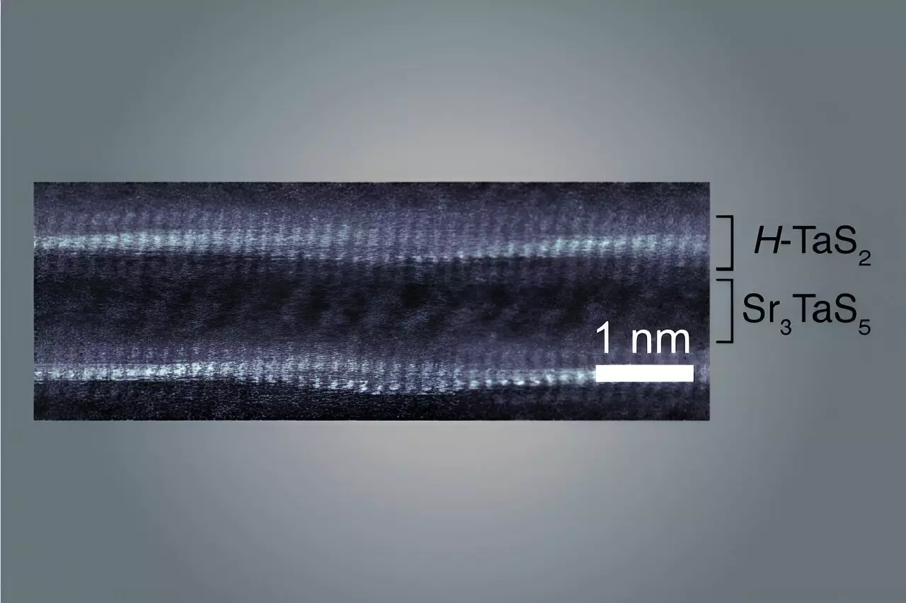
The wavy material recently synthesized at MIT serves as the second member of a burgeoning classification of compounds, following the team’s initial accomplishments in 2020 and 2021. These structures are reminiscent of a layered cake, wherein a metallic layer—comprising tantalum and sulfur—interleaves with spacer layers made of strontium, tantalum, and sulfur. The systematic stacking of these layers produces a repeat unit that spans thousands of iterations, fostering a homogeneous crystalline structure.
The fascinating aspect of this new material lies in the genesis of its ‘wavy’ architecture, which stems from the inherent mismatch in the crystal lattice dimensions of the different layers. As one layer seeks to conform to another’s structure, it buckles—creating an undulating form that dramatically influences the material’s electrical properties. The analogy of placing disparate sheets of paper conveys the challenge of arranging these differing layers while acknowledging the prevailing role of their wave formations in facilitating electron movement.
The implications of the wavy structures extend beyond their composition; they fundamentally alter electron dynamics. Once the material reaches a specific temperature, it transitions into a superconducting state characterized by the remarkable ability of electrons to traverse without resistance. Crucially, as Devarakonda, an alumni of MIT, articulates, the electrons in this material mirror the fluctuation of the structural waveforms, producing areas of varied superconductivity strength.
Moreover, the directionality imparted by the wavy structure enables electrons to navigate more efficiently down the troughs than attempt ascent over the wave crests. This directional facilitation enhances metallic properties, advocating for the wavy material’s potential utility across practical applications. The collaborative efforts of researchers at MIT reveal a commitment to pioneering a new array of materials poised to transform the landscape of conductivity and superconductivity.
With this discovery, the research team signals the dawn of new opportunities, as articulated by Devarakonda: “We’ve planted the flag; now we and others can run with applications.” By harnessing the concepts of wave formations and their resulting impacts on electron behavior, scientists are venturing into a remarkable realm of materials science, rife with possibilities.
As the landscape of superconducting materials continues to evolve, the findings from MIT encourage a bold exploration into what lies ahead. The study not only opens doors for further investigations into wave-based materials but also emphasizes the exciting prospects inherent in unexpected scientific discoveries. As more researchers delve into this uncharted territory, the realm of materials science is bound to unveil new phenomena that could redefine technological capabilities, ultimately enhancing our understanding of both fundamental and applied physics.