Antiferromagnetic materials display unique magnetic properties due to the antiparallel alignment of adjacent atomic spins, canceling out any net magnetism. This characteristic positions them as significant players in the evolving field of spintronics, which focuses on utilizing electron spin in addition to charge to enhance device performance. Antiferromagnets can potentially enable more efficient and compact electronic components due to their features of low magnetic interference and robust thermal stability. They create an impetus for research aimed at incorporating these materials into next-generation technology.
Recent developments from Harvard University have brought attention to the antiferromagnetic semiconductor MnBi2Te4, which is characterized by its centrosymmetric structure. The researchers identified an innovative phenomenon termed the antiferromagnetic diode effect within this material. Unlike typical diodes, which exhibit asymmetric charge behavior, the antiferromagnetic diode manifests a distinct kind of charge transport that exists without a net directional charge separation, a pivotal difference with significant technological implications. The findings, documented in Nature Electronics, open avenues for innovative applications in electronics.
Applications and Implications of the Diode Effect
The diode effect, a well-known concept that allows current to flow preferentially in one direction, has had applications across various electronic devices such as radio receivers, microwave circuits, and digital systems. The novelty of observing such an effect in an antiferromagnetic context expands the possibilities significantly. The Harvard team has cleverly positioned this diode effect as a core feature that could be exploited in developing advanced technologies like in-plane field effect transistors (FETs) and efficient microwave energy harvesting devices.
Analytically, the ability to harness the antiferromagnetic diode effect offers a transition from traditional semiconductor materials to more reliable, high-performance alternatives that promise improved energy efficiency and operational capabilities. As the demand for more sophisticated electronic applications grows, so does the significance of harnessing such unique materials.
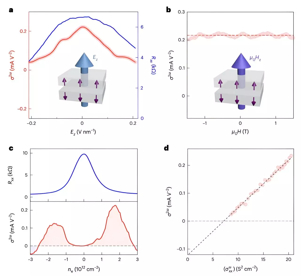
Methodology: Crafting New Devices
The process employed by the researchers was comprehensive and ingenious. They constructed various device architectures using even-layered MnBi2Te4, testing different electrode arrangements to observe the diode effect. One set of experiments used Hall bar electrodes to measure the Hall effect, while another configuration incorporated radial electrodes. This multifaceted approach allowed the researchers to explore the nonlinear transport properties inherent in their devices comprehensively.
Measurements taken during the experiments corroborated the presence of the antiferromagnetic diode effect, confirming that this behavior aligns with theoretical predictions. The innovative use of techniques like spatially resolved optical methods and electrical sum frequency generation (SFG) not only substantiated their findings but also created a methodology that could be replicated in future research on quantum materials. This opens a gateway for further exploration of nonlinear dynamics in material physics.
The implications of demonstrating the antiferromagnetic diode effect are monumental for future technologies. The researchers posit that this novel effect can inspire the creation of antiferromagnetic logic circuits and advanced microwave energy devices, contributing significantly to the field of spintronics. Their work provides a foundational framework that other scientists and engineers can further investigate to establish new devices that outperform traditional semiconductor technology significantly.
The exploration of antiferromagnetic materials like MnBi2Te4 is set to redefine our understanding and utilization of spintronic devices. As the domain advances, it is not only the antiferromagnetic diode effect that stands out but also the innovative techniques and multifaceted approaches that can pave the way for new materials to emerge. Ensuring continuous research in this area will undeniably influence the future landscape of electronic devices, facilitating the next wave of high performing, energy-efficient technology.