In today’s digital age, the demand for supercomputers has skyrocketed, leading to an alarming spike in energy expenditure. Current supercomputing infrastructures consume energy comparable to thousands of households, escalating concerns over sustainability and operational costs. This unprecedented energy consumption necessitates an urgent rethinking of how we approach computational technology. As researchers and engineers grapple with these challenges, innovative solutions are emerging. One such innovation lies within the realm of artificial neural networks and a lesser-known phenomenon known as charge density waves, which together hold the promise of a new era in energy-efficient computation.
The Promise of Neural Networks
Artificial neural networks, designed to emulate the human brain’s neuronal activities, offer exciting possibilities for energy-efficient computations. By simulating neuron-like behavior, these networks can process information in ways that were previously unattainable, transforming various fields from machine learning to complex data analysis. The ability of neural networks to operate with considerably lower power consumption compared to conventional methods presents a tantalizing opportunity that researchers are keen to explore further.
In this context, charge density waves—characterized by coordinated movements of electrons—are gaining traction as an avenue for enhancing neural networks’ functionality. The manipulation of these waves, which increase resistance and influence electron movement, could pave the way for a computing model that is both rapid and energy-efficient. The scientific community is beginning to scratch the surface of how these waves could revolutionize microelectronic devices.
Decoding Charge Density Waves
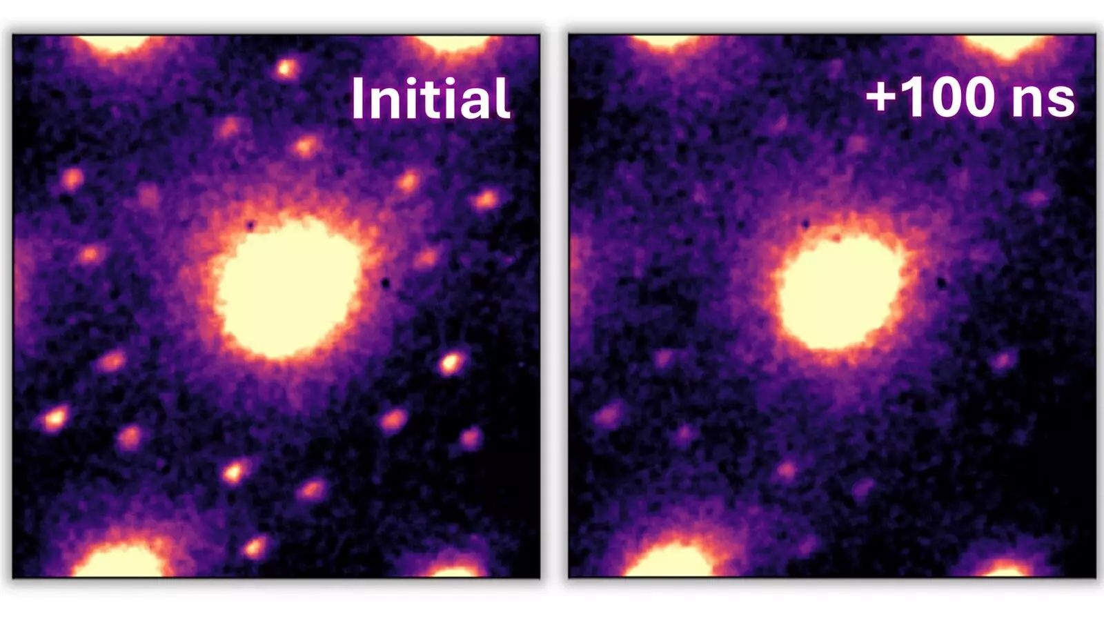
The mechanics behind charge density waves have always intrigued physicists, yet their swift transitions—occurring within mere 20 billionths of a second—pose significant challenges for research. The recent recommendations emerging from the Argonne National Laboratory underline how we can harness the potential of these waves. Adopting an innovative ultrafast electron microscope has shed light on previously elusive parameters governing these phenomena. This advancement not only underscores the importance of technological innovation in scientific exploration but also highlights the interconnectedness between experimental equipment and groundbreaking discoveries.
The materials under investigation, notably tantalum sulfide (referred to as 1T-TaS2), are notable for their capacity to form charge density waves even at room temperature, presenting a unique opportunity for researchers. The introduction of electrical pulses and the resultant observations have modified the existing narrative around how these waves operate; they do not solely respond to current, but also to thermal effects and vibrational dynamics, revealing a far more complex interaction than previously understood.
The Role of Advanced Microscopy Techniques
The groundbreaking ultrafast electron microscopy technique has emerged as a game-changer in observing the nanosecond dynamics of charge density waves. By utilizing the capabilities of the Center for Nanoscale Materials, researchers can now study these waves with exceptional precision. The groundbreaking findings illustrate that the interaction between electric currents and these waves is more intricate than anticipated. The understanding that these waves can “melt” in response to heat rather than electrical stimuli broadens the scope of how scientists conceptualize electron behavior and opens doors for enhancing microelectronic efficiency.
Understanding the vibrational manipulations that accompany these waves, akin to the neuronal signals in the brain, reflects a creative intersection of physics and cognitive science. The implication that charge density waves could generate neuron-like firing signals gives credence to the prospect of integrating physics with advanced AI architectures, infusing them with greater adaptability and efficiency.
A Forward-Looking Perspective
Researchers like Daniel Durham and Charudatta Phatak are leading the charge toward a more profound understanding of these phenomena. Their contributions not only represent a leap forward in processing capabilities but also signal a broader trend toward energy-efficient designs in microelectronics. The excitement around 1T-TaS2 as a nanoscale material suggests its potential role in future computing devices, wherein energy consumption and performance efficiency will no longer stand at odds.
As the scientific community delves deeper into the investigations surrounding charge density waves and ultrafast electron microscopy, the potential applications are poised to be transformative. With each discovery, researchers inch closer to not just optimizing supercomputers but potentially redefining the very nature of computation and machine efficiency. As the demand for sustainable technological advancement persists, the fusion of these innovative ideas will be vital to navigating the continuing energy crisis in computation today.