In a groundbreaking study published in *Nature Communications*, researchers from the Department of Energy’s Lawrence Berkeley National Laboratory and partner institutions, including Dartmouth College and Penn State, have showcased a novel strategy that promises to transform the search for materials destined for quantum applications. By employing an advanced computational approach, scientists are now able to sift through hundreds of potential materials and home in on a select few that exhibit extraordinarily promising properties for applications in quantum information science. This method represents a radical shift from traditional techniques that have largely depended on trial and error.
Alex Weber-Bargioni, a leading investigator from Berkeley Lab’s Molecular Foundry, emphasized the power of combining theoretical predictions with precise fabrication techniques. The synergy between computational screening and meticulous atomic-scale engineering not only accelerates the materials discovery process but also inspires a new generation of quantum technologies that could revolutionize computing and telecommunications, as well as enhance sensor capabilities.
The Importance of Quantum Defects
Central to the functionality of quantum materials are “defects”—imperfections within a material’s structure that can be strategically engineered to yield specific electronic properties. These quantum defects can be incorporated into systems for encoding, processing, and transmitting information on a quantum scale. However, discovering defects with optimal properties is notoriously complex. According to Geoffroy Hautier of Dartmouth, specific types of defects must possess unique abilities to absorb and emit light in relevant wavelengths for quantum applications to be feasible.
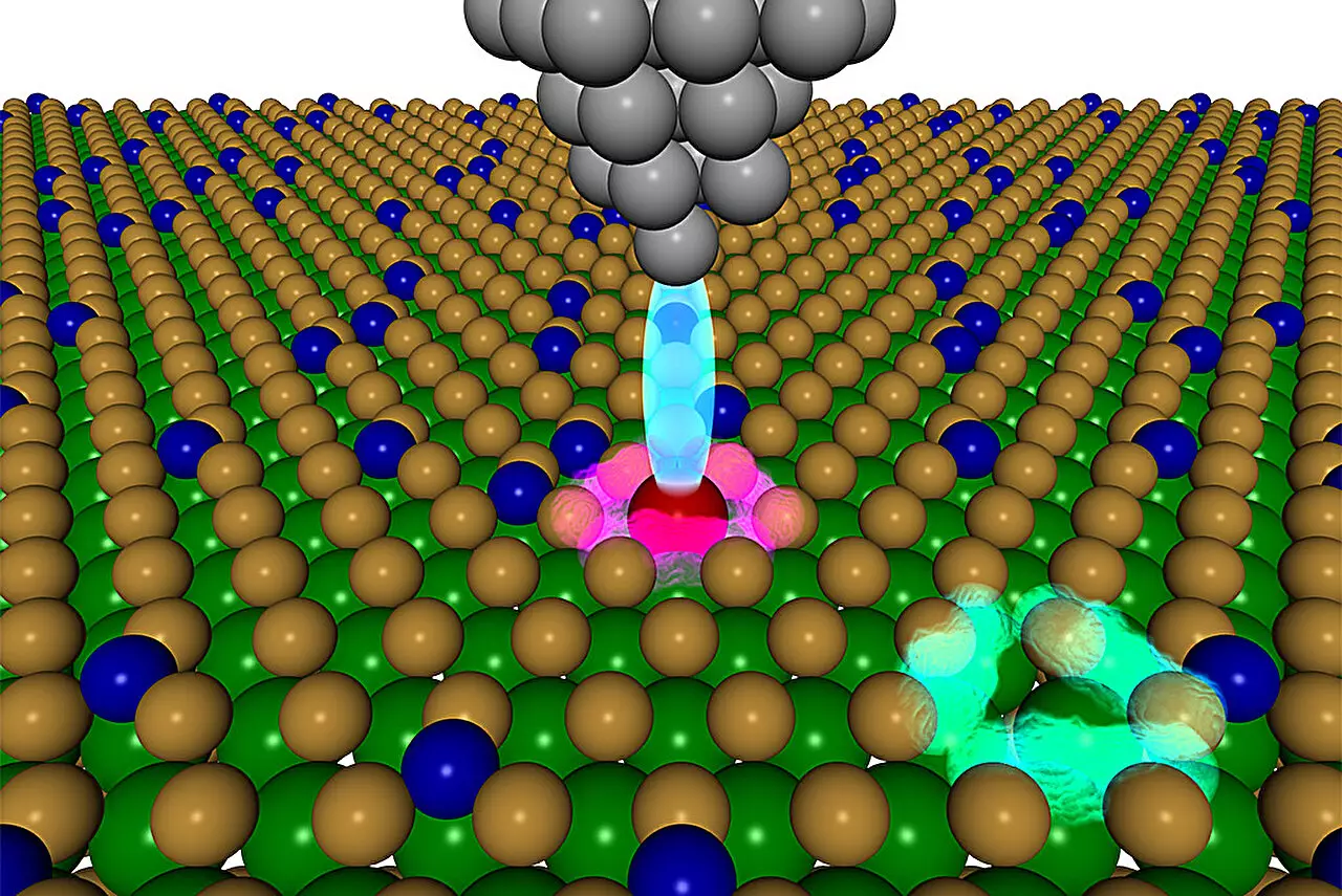
Two-dimensional (2D) materials, such as tungsten disulfide (WS2), have emerged as promising hosts for these high-quality quantum defects due to their highly tunable electronic properties. The challenge arises when researchers consider the myriad possibilities for substitutions within such materials; the potential combinations are virtually limitless, making the discovery of useful defects a daunting, time-consuming task.
Transforming Traditional Techniques
Historically, the discovery of functional quantum defects has been a slow and arduous venture, heavily reliant on experimental fabrication followed by evaluation. This trial-and-error methodology can take decades when considering even a small number of materials and defects. However, the research team ingeniously reversed this process by applying computational theory first to identify the most viable candidates, thereby significantly narrowing the scope for subsequent experimental validation.
Utilizing advanced high-throughput computational techniques, the team evaluated over 750 defects in WS2, employing substitutions of atoms within its lattice structure to predict stability, electronic composition, and light interaction properties. This meticulous computational groundwork leveraged high-performance computing capabilities to push the boundaries of material discovery and pinpoint a defect—substituting a sulfur atom with cobalt—that was previously unrecognized for its beneficial properties.
Precision Fabrication: A Game Changer
The transition from theory to practical application necessitated an innovative approach to fabrication, specifically to ensure precise placement of the identified defects. At Berkeley Lab’s Molecular Foundry, researchers have developed a refined technique that affords atomically precise manipulation of materials. By implementing specialized ion bombardment and employing scanning tunneling microscopy, scientists can create defects at specific locations, which is essential for facilitating interactions among defect sites—an important factor for their performance in quantum applications.
This capability to control the atomic-level structuring signifies a monumental advancement in the engineering of quantum materials. As John Thomas, a postdoctoral researcher at the Lab, aptly articulated, the ability to “play with atoms like LEGO bricks” opens remarkable avenues for the creation of highly uniform defects necessary for quantum entanglement and effective communication systems.
Collaboration: A Key to Success
Crucial to the successful execution of this study was the intense collaboration between theorists and experimentalists who maintained continual feedback and open lines of communication. As Hautier remarked, the unifying force behind the project was the shared funding that facilitated seamless teamwork, allowing researchers to align their methodologies and optimize the study’s outcomes.
This collective effort not only underscores the importance of interdisciplinary collaboration in scientific advancement but also highlights a paradigm shift in how materials science can approach complex challenges in quantum applications.
Looking Ahead: The Future of Quantum Materials
The implications of this study extend well beyond the immediate discoveries. Researchers are expanding their investigation into additional materials and defects, with aspirations to develop quantum states that can withstand disturbances from environmental vibrations. Such innovations promise to push the boundaries of what is possible within quantum information science.
Weber-Bargioni aptly summarized the future of this research: the ability to precisely engineer materials, driven by theoretical insight, could lead to functionalities that have not yet even been conceived. The marriage of computational prowess and hands-on experimentation beckons a new era in material science, paving the way for unprecedented applications in quantum technology.